![]()
KiCad is the open source standard for PCB design and these days a prerequisite for cheap professional PCB manufacture. I’m learning this tool out of necessity; the ultimate goal is to create a breakout board for a TSOP-50 (50-pin Thin Small Outline Package format) mask ROM chip located on a Franklin Bookman II device containing its onboard firmware in order to further my reverse engineering efforts on the system.
Once this board is created, it can be ordered through PCBWay, JLPCB, ALLPCB or any budget professional small-scale PCB manufacturer. This is likely the simplest project that we can undertake; a “hello world” of PCB design which is both useful and a realistic goal for a first stab.
With these end results in mind, let’s begin:
Part A: Logical chip design
-
We’ll be using KiCad 6.0.0 (released 2021-12-15), download and install it for your OS from https://www.kicad.org/
-
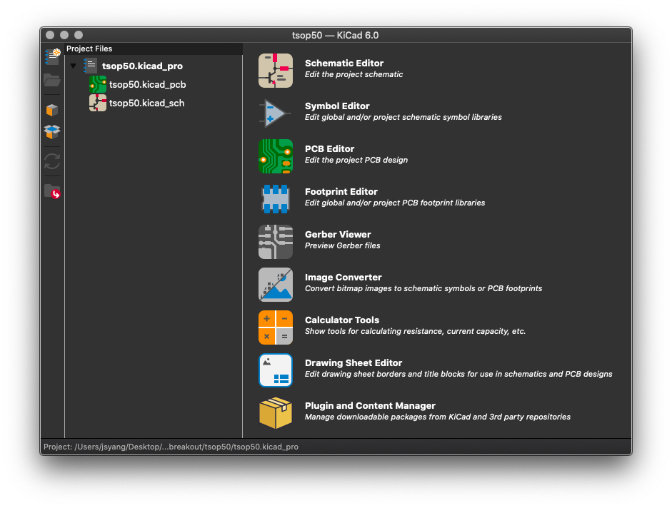
Open up KiCad and via menus:
File > New ProjectThen create a folder to contain the new project files:tsop50breakout
-
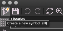
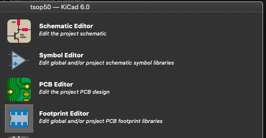
Open the “Symbol Editor”.
-
Select the “Memory_ROM” item in the library list on the left.
-
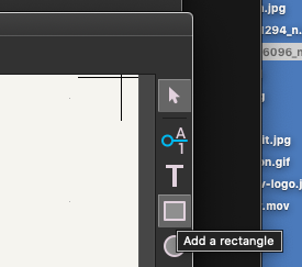
Then in the editor toolbar (top left) click on the New Symbol icon
-
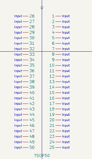
Name this symbol
TSOP50 -
There should now be 2 lines of text on top of each other: “TSOP50” and “U”. Move the mouse cursor over this text and press M on the keyboard (for move) then move the mouse cursor to a new location where the text will be translated.
-
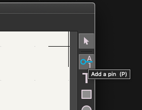
On the right hand side toolbar, click on the “Add a pin (P)” icon to add our chip’s pins
-
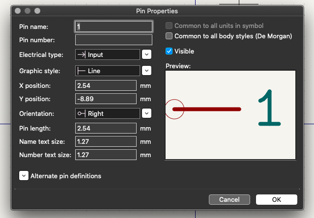
Name this pin “1”
-
Duplicate the pin 25 times per side with the Cmd-D hotkey, renaming each pin an increasing number for its new name: e.g. 2, 3, 4, …, 48, 49, 50
-
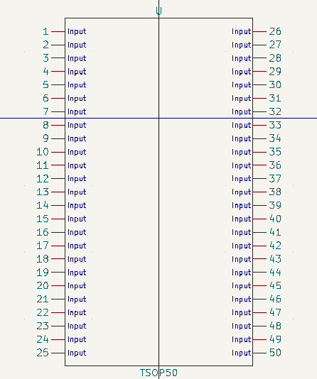
Select a bank of 25 pins and use the “Flip selected items from left to right (X)”, make sure to align the pins so that the word “Input” is facing toward the center of the chip in the final pin orientation.
-
Draw the chip body with the Rectangle tool and you should end up with something like this:
-
Click the floppy disk icon in the top left toolbar to “Save all changes”.
You are now done creating this custom symbol. Store it in your library under “Memory_ROM”. The logical chip design has been completed.
Part B: Footprint Editor
- Open the Footprint Editor
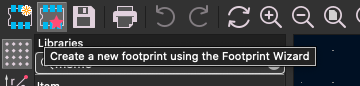
- In the top left toolbar click on the “Create a new footprint using the Footprint Wizard”
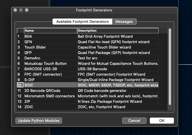
- Select the “SOIC” (10) Footprint Generator, which will take in some parameters you can set to generate a template footprint
- In the parameters table, change to these values, leaving others as defaults:
- pad count = 50
- pad length = 8 mm
- row spacing = 16 mm
(this sets the space between the rows as being at most 16mm apart)
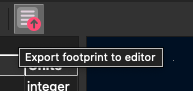
- Click on the “Export footprint to editor” to export this chip footprint!
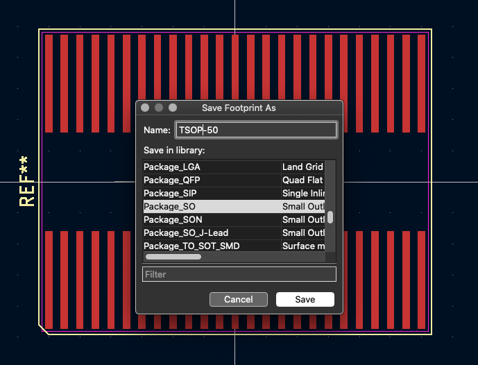
- Once back inside the main Footprint Editor, save the footprint by clicking on the floppy disk icon and then saving it within the “Package_SO” library as “TSOP-50”
You will notice this is very similar to the existing “TSOP-II-54_22.2x10.16mm_P0.8mm” footprint, which is exactly as intended. With only 50 pins, we would not require the extra 4 but can use this as a backup footprint for manufacturing.
Part C: Schematic Editor
-
Open the schematic and insert the “TSOP-50” symbol into it that you created from Part A
-
Add 2 x “Conn 01x25” generic connector symbols to the schematic diagram
-
Double click on each of the three components in your schematic And ensure they have footprints tied to them from the symbol library
- J1 (1 x 25 connector) should be tied to
- J2 (1 x 25 connector)
- U1 (TSOP-50)
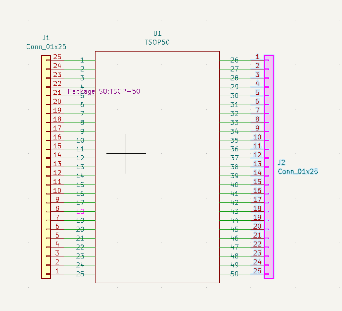
- Ensure all the pins / traces of the components are linked to one another with traces
- Save the schematic and exit the editor.
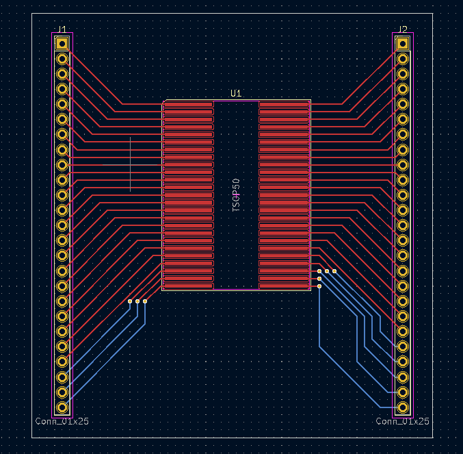
Part D: PCB Editor
-
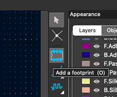
Either use the schematic created from Part C … OR insert the footprints manually with the “Add a footprint” icon
-
Once the component footprints are in, you can draw the traces with the “Route tracks (x)” tool
-
Using the V key, you can choose to route traces through vias so they can make use of the underside of the PCB
-
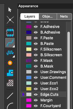
Once components and traces are all laid out accordingly, you can draw a rectangular (or other shape) bound to indicate the main PCB body. Use the “Edge.Cuts” layer for this. It is usually in yellow.
-
Once your PCB has been drawn, you can also view it in 3D via “View > 3D Viewer”
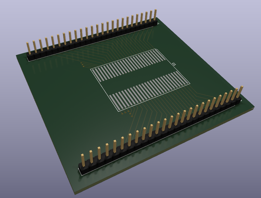
The breakout board is now complete!